| CPC H01L 23/562 (2013.01) [H01L 23/481 (2013.01); H01L 23/5226 (2013.01); H01L 23/528 (2013.01); H01L 23/585 (2013.01); H01L 21/78 (2013.01)] | 6 Claims |
|
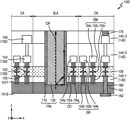
1. A semiconductor device, comprising:
a semiconductor substrate including a chip area and a first scribe lane area;
a low-k layer on the semiconductor substrate;
a first trench area in the first scribe lane area, the first trench area comprising a trench;
an interlayer insulating layer on the low-k layer;
a first metal liner in the first scribe lane area, the first metal liner extending vertically and continuously from the semiconductor substrate through the low-k layer and the interlayer insulating layer along a sidewall of the trench; and
a first gap-fill insulating layer in the first trench area and vertically extending from the semiconductor substrate through the low-k layer and the interlayer insulating layer to expose an upper surface of the first gap-fill insulating layer through the interlayer insulating layer,
wherein the first metal liner covers a side surface of the first gap-fill insulating layer and is disposed between the first gap-fill insulating layer and the low-k layer and between the first gap-fill insulating layer and the interlayer insulating layer, and
wherein a lower surface of the first gap-fill insulating layer contacts the semiconductor substrate.
|