US 12,230,585 B2
Photolithography alignment process for bonded wafers
Yeong-Jyh Lin, Caotun Township (TW); Ching I Li, Tainan (TW); De-Yang Chiou, Hsinchu (TW); Sz-Fan Chen, Kaohsiung (TW); Han-Jui Hu, Tainan (TW); Ching-Hung Wang, Hsinchu (TW); Ru-Liang Lee, Hsinchu (TW); and Chung-Yi Yu, Hsin-Chu (TW)
Assigned to Taiwan Semiconductor Manufacturing Company, Ltd., Hsinchu (TW)
Filed by Taiwan Semiconductor Manufacturing Company, Ltd., Hsin-Chu (TW)
Filed on Jan. 24, 2024, as Appl. No. 18/420,972.
Application 17/834,235 is a division of application No. 17/062,677, filed on Oct. 5, 2020, granted, now 11,362,038, issued on Jun. 14, 2022.
Application 18/420,972 is a continuation of application No. 17/834,235, filed on Jun. 7, 2022, granted, now 11,916,022.
Claims priority of provisional application 63/030,990, filed on May 28, 2020.
Prior Publication US 2024/0186258 A1, Jun. 6, 2024
This patent is subject to a terminal disclaimer.
Int. Cl. H01L 21/683 (2006.01); G03F 1/42 (2012.01); G03F 1/70 (2012.01); H01L 21/027 (2006.01); H01L 21/66 (2006.01); H01L 23/544 (2006.01)
CPC H01L 23/544 (2013.01) [G03F 1/42 (2013.01); G03F 1/70 (2013.01); H01L 21/0274 (2013.01); H01L 21/6835 (2013.01); H01L 22/20 (2013.01); H01L 2221/68309 (2013.01); H01L 2223/54426 (2013.01)] 20 Claims
OG exemplary drawing
 
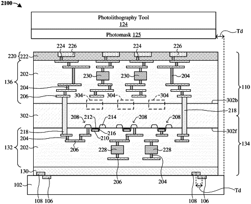
1. A method for forming an integrated chip, comprising:
performing an alignment process on a first semiconductor workpiece and a second semiconductor workpiece by virtue of a plurality of workpiece pins;
bonding the first semiconductor workpiece to the second semiconductor workpiece;
determining a shift value between the first and second semiconductor workpieces by virtue of a first plurality of alignment marks on the first semiconductor workpiece and a second plurality of alignment marks on the second semiconductor workpiece; and
forming a layer of an integrated circuit (IC) structure over the second semiconductor workpiece based at least in part on the shift value.