| CPC H01L 23/5386 (2013.01) [H01L 23/49816 (2013.01); H01L 23/49833 (2013.01); H01L 23/49838 (2013.01); H01L 23/5385 (2013.01); H01L 24/16 (2013.01); H01L 25/162 (2013.01); H01L 2224/16225 (2013.01)] | 13 Claims |
|
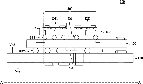
1. A semiconductor chiplet device, comprising:
a first die comprising a first interface, wherein the first interface has a plurality of first power nodes;
a second die comprising a second interface, wherein the second interface has a plurality of second power nodes;
an interposer layer comprising a first side and a second side corresponding to the first side of the interposer layer, wherein the first side of the interposer layer is configured to set the first die and the second die to couple to the first die and the second die, the first die and the second die are configured to perform a data transmission through the first interface, the interposer layer and the second interface;
a package substrate arranged on the second side of the interposer layer, and comprising a first side and a second side corresponding to the first side of the package substrate, wherein the first side of the package substrate is coupled to the second side of the interposer layer through a plurality of first bumps and a plurality of second bumps, the plurality of first bumps is coupled to the plurality of first power nodes through the interposer layer, and the plurality of second bumps is coupled to the plurality of second power nodes through the interposer layer;
a plurality of third bumps arranged on the second side of the package substrate, and coupled to the plurality of first bumps through the package substrate;
a plurality of fourth bumps arranged on the second side of the package substrate, and coupled to the plurality of second bumps through the package substrate;
a first decoupling capacitor arranged on the second side of the package substrate, wherein the first decoupling capacitor is arranged between the plurality of third bumps, and is arranged in a first vertical projection area of the first interface on the package substrate; and
a second decoupling capacitor arranged on the second side of the package substrate, wherein the second decoupling capacitor is arranged between the plurality of fourth bumps, and is arranged in a second vertical projection area of the second interface on the package substrate.
|