US 12,230,572 B2
Backside signal interconnection
Yu-Xuan Huang, Hsinchu (TW); Ching-Wei Tsai, Hsinchu (TW); Yi-Hsun Chiu, Hsinchu County (TW); Yi-Bo Liao, Hsinchu (TW); Kuan-Lun Cheng, Hsin-Chu (TW); Wei-Cheng Lin, Taichung (TW); Wei-An Lai, Hsinchu (TW); Ming Chian Tsai, Hsinchu (TW); Jiann-Tyng Tzeng, Hsin Chu (TW); Hou-Yu Chen, Hsinchu County (TW); Chun-Yuan Chen, Hsinchu (TW); and Huan-Chieh Su, Changhua County (TW)
Assigned to TAIWAN SEMICONDUCTOR MANUFACTURING COMPANY, LTD., Hsinchu (TW)
Filed by Taiwan Semiconductor Manufacturing Company, Ltd., Hsin-Chu (TW)
Filed on May 18, 2023, as Appl. No. 18/319,593.
Application 18/319,593 is a division of application No. 17/196,174, filed on Mar. 9, 2021, granted, now 11,658,119.
Claims priority of provisional application 63/106,264, filed on Oct. 27, 2020.
Prior Publication US 2023/0307365 A1, Sep. 28, 2023
Int. Cl. H01L 23/528 (2006.01); H01L 21/768 (2006.01); H01L 23/522 (2006.01); H01L 27/088 (2006.01); H01L 29/06 (2006.01); H01L 29/78 (2006.01)
CPC H01L 23/5286 (2013.01) [H01L 21/76838 (2013.01); H01L 23/5226 (2013.01); H01L 27/088 (2013.01); H01L 29/0649 (2013.01); H01L 29/78 (2013.01)] 20 Claims
OG exemplary drawing
 
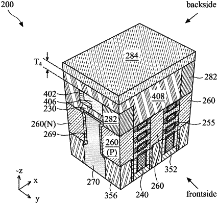
1. A semiconductor structure, comprising:
a first transistor having a first source/drain (S/D) feature and a first gate;
a second transistor having a second S/D feature and a second gate;
a multi-layer interconnection disposed over the first and the second transistors;
a signal interconnection under the first and the second transistors; and
a power rail under the signal interconnection and electrically isolated from the signal interconnection, wherein the signal interconnection electrically connects one of the first S/D feature and the first gate to one of the second S/D feature and the second gate.