| CPC H01L 23/5283 (2013.01) [H01L 21/76805 (2013.01); H01L 21/76816 (2013.01); H01L 21/76846 (2013.01); H01L 21/76852 (2013.01); H01L 21/76871 (2013.01); H01L 21/76895 (2013.01); H01L 23/535 (2013.01)] | 20 Claims |
|
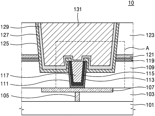
1. A method of manufacturing an interconnection structure of an integrated circuit semiconductor device, the method comprising:
forming a first conductive layer on a semiconductor substrate;
forming an interlayer insulating layer and a via layer on the first conductive layer, the via layer contacting the first conductive layer;
forming a trench in the interlayer insulating layer to expose the via layer, the trench being recessed from a top surface of the interlayer insulating layer;
forming a barrier film selectively on a bottom of the trench, sidewalls of the trench, and sidewalls of the via layer in the trench, such that the barrier film is not formed in contact with a top surface of the via layer during the forming the barrier film, the barrier film exposing the top surface of the via layer; and
forming a second conductive layer inside the trench on the barrier film, the second conductive layer being electrically connected to the first conductive layer through the via layer, wherein
the forming the barrier film selectively forms a first portion of the barrier film on the sidewalls of the trench and a second portion of the barrier film on the sidewalls of the via layer in the trench, and
the first portion of the barrier film faces the second portion of the barrier film and is laterally spaced apart from the second portion of the barrier film.
|