| CPC H01L 23/49838 (2013.01) [H01L 21/4857 (2013.01); H01L 21/486 (2013.01); H01L 23/13 (2013.01); H01L 23/49822 (2013.01); H01L 23/49866 (2013.01); H01L 23/5385 (2013.01); H01L 23/49816 (2013.01); H01L 23/5383 (2013.01); H01L 2224/16225 (2013.01); H01L 2924/15311 (2013.01)] | 21 Claims |
|
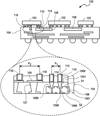
1. A semiconductor device, comprising:
a first integrated circuit die, the first integrated circuit die having a first die interconnect structure and a second die interconnect structure;
a second integrated circuit die adjacent and laterally spaced from the first integrated circuit die;
a substrate having a substrate top side adjacent the first integrated circuit die and second integrated circuit die, and a substrate bottom side opposite the top side, the substrate comprising:
a bridge embedded in the substrate, the bridge having a bridge top surface, a bridge bottom surface, the bridge top surface being closer to the first integrated circuit die than the bridge bottom surface is, the bridge having a bridge height measured between the bridge top surface and the bridge bottom surface, and the bridge having a first bridge contact pad at the bridge top surface;
a first bridge via extending from the first bridge contact pad away from the bridge top surface, the first bridge via having a first bridge via height;
a first bridge contact extending from a top of the first bridge via towards the first integrated circuit die, the first bridge contact having a first width, the first bridge contact being electrically coupled to the first die interconnect structure;
a first non-bridge via laterally spaced from the embedded bridge, the first non-bridge via having a first non-bridge via height greater than the first bridge via height, wherein the first non-bridge via has a top surface above a top surface of the first bridge contact pad;
a first conductive portion of a redistribution layer above and electrically coupled to the first non-bridge via; and
a first non-bridge contact laterally spaced away from the bridge and above and electrically coupled to the first conductive portion of the redistribution layer, the first non-bridge contact positioned so that a line parallel to the bridge top surface intersects both the first bridge contact and the first non-bridge contact, the first non-bridge contact having a second width greater than the first width of the first bridge contact, the first non-bridge contact being electrically coupled to the second die interconnect structure.
|