| CPC H01L 23/49838 (2013.01) [H01L 33/62 (2013.01)] | 20 Claims |
|
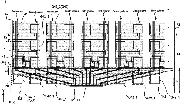
1. A light-emitting substrate, comprising:
a base;
a first conductive pattern layer disposed on the base, the first conductive pattern layer including a plurality of first signal lines; and
a second conductive pattern layer disposed on a side of the first conductive pattern layer away from the base, wherein the second conductive pattern layer includes a plurality of lamp bead pads, and the plurality of lamp bead pads include a plurality of first lamp bead pads and at least one second lamp bead pad; a vertical projection of each first lamp bead pad on the base at least partially overlaps with a vertical projection of a first signal line on the base; a vertical projection of each second lamp bead pad on the base is outside vertical projections of the plurality of first signal lines on the base;
a distance between a first lamp bead pad and the base is substantially the same as a distance between a second lamp bead pad and the base;
the light-emitting substrate has two edges opposite to each other in a first direction, and an effective light-emitting region and a fan-out region that are located between the two edges and distributed in a second direction, the first signal line includes a first portion and a second portion, the second portion is located in the fan-out region, there is an included angle between the first portion and the second portion, a distance between ends of second portions of two adjacent first signal lines that are away from first portions is smaller than a distance between the first portions of the two adjacent first signal lines, the fan-out region includes at least one first sub-region and at least one second sub-region; the second portion of each first signal line is provided in the first sub-region, at least one second lamp bead pad is provided in the second sub-region.
|