| CPC H01L 23/49822 (2013.01) [H01L 21/4853 (2013.01); H01L 21/4857 (2013.01); H01L 21/4864 (2013.01); H01L 21/568 (2013.01); H01L 21/6835 (2013.01); H01L 23/3114 (2013.01); H01L 23/3142 (2013.01); H01L 23/49816 (2013.01); H01L 23/49838 (2013.01); H01L 21/561 (2013.01); H01L 23/3128 (2013.01); H01L 23/49811 (2013.01); H01L 24/13 (2013.01); H01L 24/16 (2013.01); H01L 24/81 (2013.01); H01L 24/97 (2013.01); H01L 25/0655 (2013.01); H01L 25/50 (2013.01); H01L 2221/68345 (2013.01); H01L 2221/68359 (2013.01); H01L 2221/68381 (2013.01); H01L 2224/13111 (2013.01); H01L 2224/13144 (2013.01); H01L 2224/13155 (2013.01); H01L 2224/16238 (2013.01); H01L 2224/81005 (2013.01); H01L 2224/81192 (2013.01); H01L 2224/81805 (2013.01); H01L 2224/95001 (2013.01); H01L 2224/97 (2013.01); H01L 2924/14 (2013.01); H01L 2924/15311 (2013.01); H01L 2924/15313 (2013.01); H01L 2924/18161 (2013.01); H01L 2924/37001 (2013.01)] | 9 Claims |
|
1. A package device, comprising:
an electronic device;
a conductive pad having a first bottom surface;
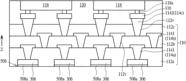
a redistribution layer disposed between the conductive pad and the electronic device, the redistribution layer having a second bottom surface, and the conductive pad being electrically connected to the electronic device through the redistribution layer, wherein the redistribution layer comprises a first insulating layer away from the electronic device, the first insulating layer has an opening, and the conductive pad is disposed in the opening;
a solder ball electrically connected to the electronic device through the conductive pad and the redistribution layer; and
a conductive element, wherein at least a portion of the conductive element is disposed between the conductive pad and the first insulating layer in a normal direction of the second bottom surface,
wherein the first bottom surface is closer to the electronic device than the second bottom surface in the normal direction of the electronic device, and a maximum width of the solder ball is less than a maximum width of the conductive pad.
|