| CPC H01L 23/49822 (2013.01) [H01L 23/3107 (2013.01); H01L 23/49816 (2013.01); H01L 23/49894 (2013.01); H01L 24/42 (2013.01); H01L 2224/48228 (2013.01)] | 20 Claims |
|
1. A semiconductor package comprising:
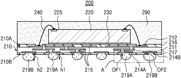
a base substrate having an upper surface on which a plurality of upper pads are arranged and a lower surface on which a plurality of first and second lower pads are arranged and including an interconnection circuit electrically connecting the plurality of upper pads and the plurality of first and second lower pads;
a semiconductor chip disposed on the upper surface of the base substrate and electrically connected to the plurality of upper pads;
a solder resist layer having a plurality of openings exposing a region of each of the plurality of first and second lower pads, the exposed regions of the plurality of first and second lower pads having substantially the same size;
a plurality of first external connection conductors respectively disposed on the exposed regions of the plurality of first lower pads, each of the first external connection conductors having a first height and a first volume; and
a plurality of second external connection conductors respectively disposed on the exposed regions of the plurality of second lower pads, each of the second external connection conductors having a second height, greater than the first height, and a second volume, greater than the first volume,
wherein a pitch of each of the plurality of first and second lower pads is substantially the same.
|