| CPC H01L 23/49811 (2013.01) [H01L 23/3128 (2013.01); H01L 23/49822 (2013.01); H01L 24/16 (2013.01); H01L 25/18 (2013.01); H01L 23/34 (2013.01); H01L 24/73 (2013.01); H01L 2224/16227 (2013.01); H01L 2224/73204 (2013.01)] | 16 Claims |
|
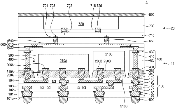
1. A semiconductor package, comprising:
a redistribution substrate;
a semiconductor chip on a top surface of the redistribution substrate; and
a solder terminal on a bottom surface of the redistribution substrate,
wherein the redistribution substrate includes:
an under-bump pattern;
a dielectric layer on a sidewall of the under-bump pattern;
an under-bump seed pattern between the dielectric layer and the sidewall of the under-bump pattern; and
a redistribution pattern on a top surface of the under-bump pattern,
wherein the solder terminal is on a bottom surface of the under-bump pattern,
wherein the bottom surface of the under-bump pattern is at a level higher than a level of a bottom surface of the dielectric layer,
wherein the under-bump seed pattern does not extend onto any of a top surface of the dielectric layer and the bottom surface of the under-bump pattern.
|