US 12,230,554 B2
Shield structure for backside through substrate vias (TSVs)
Min-Feng Kao, Chiayi (TW); Dun-Nian Yaung, Taipei (TW); Hsing-Chih Lin, Tainan (TW); Jen-Cheng Liu, Hsin-Chu (TW); and Wei-Tao Tsai, Tainan (TW)
Assigned to Taiwan Semiconductor Manufacturing Company, Ltd., Hsinchu (TW)
Filed by Taiwan Semiconductor Manufacturing Company, Ltd., Hsin-Chu (TW)
Filed on Jul. 27, 2023, as Appl. No. 18/359,996.
Application 17/355,534 is a division of application No. 16/553,222, filed on Aug. 28, 2019, granted, now 11,062,977, issued on Jul. 13, 2021.
Application 18/359,996 is a continuation of application No. 17/355,534, filed on Jun. 23, 2021, granted, now 11,764,129.
Claims priority of provisional application 62/855,274, filed on May 31, 2019.
Prior Publication US 2023/0369173 A1, Nov. 16, 2023
Int. Cl. H01L 27/02 (2006.01); H01L 21/3065 (2006.01); H01L 21/761 (2006.01); H01L 21/762 (2006.01); H01L 21/768 (2006.01); H01L 23/48 (2006.01); H01L 23/60 (2006.01); H01L 25/00 (2006.01); H01L 25/065 (2023.01); H01L 23/00 (2006.01); H01L 23/522 (2006.01); H01L 23/528 (2006.01); H01L 29/06 (2006.01); H01L 29/66 (2006.01); H01L 29/78 (2006.01)
CPC H01L 23/481 (2013.01) [H01L 21/3065 (2013.01); H01L 21/761 (2013.01); H01L 21/76224 (2013.01); H01L 21/76898 (2013.01); H01L 23/60 (2013.01); H01L 25/0657 (2013.01); H01L 25/50 (2013.01); H01L 27/0255 (2013.01); H01L 27/0296 (2013.01); H01L 23/5226 (2013.01); H01L 23/5283 (2013.01); H01L 24/05 (2013.01); H01L 24/08 (2013.01); H01L 24/80 (2013.01); H01L 29/0653 (2013.01); H01L 29/66689 (2013.01); H01L 29/7816 (2013.01); H01L 2224/05571 (2013.01); H01L 2224/08147 (2013.01); H01L 2224/80357 (2013.01); H01L 2224/80895 (2013.01); H01L 2224/80896 (2013.01); H01L 2225/06544 (2013.01)] 20 Claims
OG exemplary drawing
 
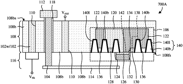
1. An integrated circuit (IC) comprising:
a semiconductor substrate;
a semiconductor device on and partially defined by the semiconductor substrate;
a through substrate via (TSV) extending through the semiconductor substrate; and
a semiconductor shield structure extending completely through the semiconductor substrate, wherein the semiconductor shield structure is between the semiconductor device and the TSV and confines free radicals at the TSV to between the TSV and the semiconductor shield structure.