| CPC H01L 22/12 (2013.01) [G03F 7/70633 (2013.01); G03F 7/70655 (2023.05); H01L 21/302 (2013.01); H01L 21/682 (2013.01); H01L 23/544 (2013.01); H01L 2223/54426 (2013.01)] | 20 Claims |

|
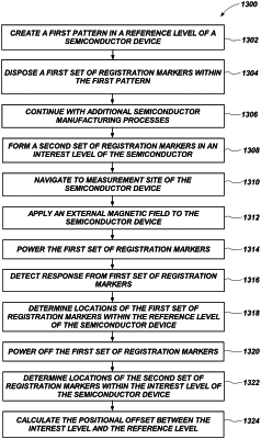
1. A registration system, comprising:
a substrate support for supporting a wafer;
an optical microscope imaging or scatterometry system configured to recognize at least locations of visible elements on a wafer;
a sensor movable over the wafer and configured to detect magnetic attributes of non-visible elements of the wafer; and
a controller operably coupled to the substrate support, the sensor and the optical microscope imaging or scatterometry system, the controller comprising:
at least one processor; and
at least one non-transitory computer-readable storage medium storing instructions thereon that, when executed by the at least one processor, cause the controller to:
receive data related to detected magnetic attributes of the non-visible elements from the sensor;
responsive to the received data related to detected magnetic attributes, determine at least locations of the non-visible elements within the wafer;
receive date related to recognized at least locations of visible elements on a wafer;
responsive to the received data related to recognized at least locations of visible elements, determine at least locations of the visible elements on the wafer; and
responsive to a determined at least locations of at least one non-visible element and at least one visible element, calculate a positional offset between the at least one non-visible element and the at least one visible element.
|