| CPC H01L 21/7682 (2013.01) [H01L 21/76829 (2013.01); H01L 21/76831 (2013.01); H01L 21/76832 (2013.01); H01L 21/76837 (2013.01); H01L 21/76846 (2013.01); H01L 21/76877 (2013.01); H01L 23/5226 (2013.01)] | 20 Claims |
|
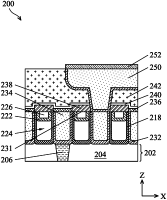
18. A method for forming an interconnect structure, comprising:
forming a first conductive feature in a dielectric layer;
forming a first conductive layer over the dielectric layer;
forming one or more openings in the first conductive layer to expose portions of the dielectric layer;
forming a capping layer on exposed surfaces of the first conductive layer and the dielectric layer;
forming a sacrificial layer on the capping layer in the one or more openings;
forming a support layer on the sacrificial layer and the capping layer in the one or more openings;
removing the sacrificial layer to form an air gap in the one or more openings;
forming a dielectric fill on the support layer;
replacing the first conductive layer with a second conductive layer;
performing a planarization process so that surfaces of the second conductive layer are substantially co-planar with top surfaces of the dielectric fill, the support layer, the capping layer, and the dielectric fill; and
selectively forming a two-dimensional (2D) material layer on the second conductive layer.
|