| CPC H01L 21/302 (2013.01) [H01L 21/48 (2013.01); H01L 21/561 (2013.01); H01L 21/565 (2013.01); H01L 21/78 (2013.01); H01L 23/12 (2013.01); H01L 23/3185 (2013.01); H01L 24/04 (2013.01); H01L 24/26 (2013.01); H01L 2224/94 (2013.01)] | 12 Claims |
|
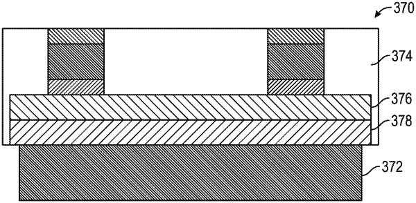
1. A semiconductor package, comprising:
a semiconductor die comprising a first side and a second side, the first side of the semiconductor die comprising one or more electrical contacts;
a layer of metal coupled directly to the second side of the semiconductor die; and
only a single stress balance structure coupled directly to and around the one or more electrical contacts,
wherein the single stress balance structure is a continuously formed structure;
wherein the semiconductor die comprises a thickness between 0.1 microns and 125 microns; and
wherein the single stress balance structure is directly coupled to only the semiconductor die at the first side and a plurality of sidewalls.
|