| CPC H01H 50/546 (2013.01) [H01H 50/12 (2013.01); H01H 51/29 (2013.01); H01H 2225/004 (2013.01); H01H 2225/008 (2013.01)] | 10 Claims |
|
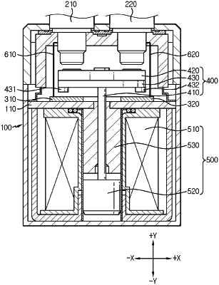
1. A relay switch device that turns on/off a current flow on a current transmission line, the relay switch device comprising:
a relay housing forming an exterior of the relay switch device;
a first upper fixing terminal and a second upper fixing terminal arranged side by side and separated by a fixed distance, and extending through the relay housing;
a first lower fixing terminal electrically connected to the first upper fixing terminal and arranged under the first upper fixing terminal and separated by a predetermined distance from the first upper fixing terminal;
a second lower fixing terminal electrically connected to the second upper fixing terminal and arranged under the second upper fixing terminal and separated by the predetermined distance from the second upper fixing terminal; and
a circuit mode switch module configured to be moveable by a predetermined distance and to selectively contact the first and second upper fixing terminals or the first and second lower fixing terminals,
wherein node voltages in the first upper fixing terminal and the second upper fixing terminal are made substantially equal in response to the circuit mode switch module contacting the first and second upper fixing terminals, and
wherein the node voltages in the first upper fixing terminal and the second upper fixing terminal are made substantially different in response to the circuit mode switch module contacting the first and second lower fixing terminals.
|