| CPC H01H 1/0036 (2013.01) [H01H 1/06 (2013.01); H01H 11/00 (2013.01); H01H 11/06 (2013.01); H01H 59/0009 (2013.01); H01H 2001/0057 (2013.01); H01H 2001/0078 (2013.01); H01L 21/32051 (2013.01); H01L 21/76224 (2013.01)] | 12 Claims |

|
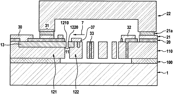
1. A method for manufacturing a MEMS switch that includes at least one embedded metal contact, including the following steps:
A) providing a substrate, wherein a silicon layer is situated on the substrate;
B) introducing narrow trenches into the silicon layer using anisotropic etching;
C) filling the narrow trenches by deposition of a first metal layer;
D) removing the first metal layer at a surface of the silicon layer, the first metal layer remaining in the narrow trenches and thus creating at least one embedded metal contact;
H) structuring the silicon layer via a trenching process, a fixed portion and a switching element being formed, and a contact area of the at least one embedded metal contact being exposed with respect to the silicon layer,
wherein the contact area includes a first contact area and an oppositely situated second contact area, wherein the first contact area and the second contact area are exposed with respect to the silicon layer,
wherein the first metal layer is situated at a side of the silicon layer facing away from the substrate.
|
|
8. A method for manufacturing a MEMS switch that includes at least one embedded metal contact, including the following steps:
A) providing a substrate that includes a silicon layer;
B) introducing narrow trenches into the silicon layer using anisotropic etching;
C) filling the narrow trenches by deposition of a first metal layer;
D) removing the first metal layer at a surface of the silicon layer, the first metal layer remaining in the narrow trenches and thus creating at least one embedded metal contact;
H) structuring the silicon layer via a trenching process, a fixed portion and a switching element being formed, and a contact area of the at least one embedded metal contact being exposed with respect to the silicon layer,
wherein the contact area includes a first contact area and an oppositely situated second contact area, wherein the first contact area and the second contact area are exposed with respect to the silicon layer,
wherein a substrate including a first insulating layer and the silicon layer is provided in step A, and after step H, the first insulating layer is etched below a structured area of the silicon layer in a step I, the switching element being exposed and made movable.
|