| CPC H01G 4/30 (2013.01) [H01G 4/012 (2013.01); H01G 4/33 (2013.01); H01L 28/60 (2013.01); H01L 28/92 (2013.01)] | 8 Claims |
|
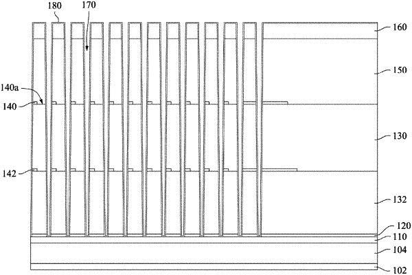
1. A semiconductor structure, comprising:
a landing pad layer;
a middle patterned dielectric layer disposed over the landing pad layer, wherein the middle patterned dielectric layer comprises a plurality of first openings;
a top patterned dielectric layer disposed over the middle patterned dielectric layer, wherein the top patterned dielectric layer comprises a plurality of second openings substantially aligned with the first openings, respectively;
a bottom patterned dielectric layer disposed between the landing pad layer and the middle patterned dielectric layer, wherein the bottom patterned dielectric layer comprises a plurality of third openings substantially aligned with the first openings, respectively; and
a plurality of trench conductive layers, wherein each of the trench conductive layers is disposed through a portion of one of the second openings and a portion of one of the first openings, and each of the trench conductive layers has two side layers opposite to each other, and a height difference between a lower one of the two side layers and a lower surface of the top patterned dielectric layer is in a range of 0 to 50 nm.
|