| CPC H01G 4/30 (2013.01) [H01G 2/065 (2013.01); H01G 4/008 (2013.01); H01G 4/012 (2013.01); H01G 4/12 (2013.01); H01G 4/232 (2013.01)] | 30 Claims |
|
1. A multilayer electronic component comprising:
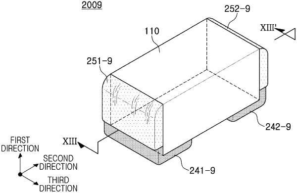
a body including a dielectric layer and first and second internal electrode alternately disposed with the dielectric layer interposed therebetween, the body having first and second surfaces opposing each other in a first direction, third and fourth surfaces connected to the first and second surfaces and opposing each other in a second direction, fifth and sixth surfaces connected to the first to fourth surfaces and opposing each other in a third direction;
a first external electrode including a first connection portion disposed on the third surface, and a first band portion extending from the first connection portion onto a first portion of the first surface;
a second external electrode including a second connection portion disposed on the fourth surface, and a second band portion extending from the second connection portion onto a second portion of the first surface;
an insulating layer including a first insulating layer disposed on the first connection portion and a second insulating layer disposed on the second connection portion;
a first plating layer disposed on the first band portion; and
a second plating layer disposed on the second band portion,
wherein the insulating layer includes BaO, a material different from barium titanate based ceramic material included in e dielectric layer.
|