| CPC G11C 7/1063 (2013.01) [G11C 7/1057 (2013.01); G11C 7/1084 (2013.01); G11C 7/222 (2013.01)] | 20 Claims |
|
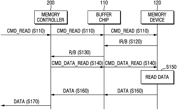
1. A memory system comprising:
a plurality of nonvolatile memory chips each including a status output pin;
a memory controller including a first pin; and
a buffer chip connected between the plurality of nonvolatile memory chips and the memory controller and including a second pin configured to output an external state signal to the first pin and a third pin configured to receive a plurality of internal state signals, which indicate states of the plurality of nonvolatile memory chips, from the status output pins,
wherein the buffer chip is configured to:
determine a duty cycle of the external state signal on the basis of identifications (IDs) of the plurality of nonvolatile memory chips which output the plurality of internal state signals, and
output the external state signal,
wherein the memory controller is configured to:
determine which of the plurality of nonvolatile memory chips is in a particular state without a status read command, and
provide an input/output command to at least one of the plurality of nonvolatile memory chips, and
wherein the input/output command includes a read command or a write command.
|