| CPC G11C 7/1042 (2013.01) [G11C 7/1012 (2013.01); G11C 7/1066 (2013.01); G11C 7/1093 (2013.01); G11C 7/22 (2013.01)] | 14 Claims |
|
1. A memory integrated circuit device, comprising:
a command/address interface to receive access commands from an external memory controller;
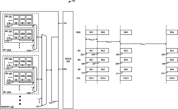
a plurality of bank group clusters;
each of the bank group clusters comprising a plurality of respective bank groups;
each of the bank groups comprising a plurality of respective memory banks;
wherein successive access commands of a first type of command that are addressed to different memory banks that are members of the same bank group of the same bank group cluster are subject to a first timing constraint for receiving, from the external memory controller, the successive access commands of the first type of command that are addressed to different memory banks that are members of the same bank group of the same bank group cluster;
successive access commands of the first type of command that are addressed to memory banks that are members of different bank groups of the same bank group cluster are subject to a second timing constraint for receiving, from the external memory controller, the successive access commands of the first type of command that are addressed to memory banks that are members of different bank groups of the same bank group cluster; and
successive access commands of the first type of command that are addressed to memory banks that are members of different bank group clusters are subject to a third timing constraint for receiving, from the external memory controller, the successive access commands of the first type of command that are addressed to memory banks that are members of different bank group clusters, wherein the first timing constraint, the second timing constraint, and the third timing constraint are all unequal minimum time delay intervals.
|