| CPC G11C 19/28 (2013.01) [G09G 3/20 (2013.01); G09G 3/3266 (2013.01); G09G 3/3677 (2013.01); G09G 2310/0267 (2013.01); G09G 2310/0286 (2013.01)] | 6 Claims |
|
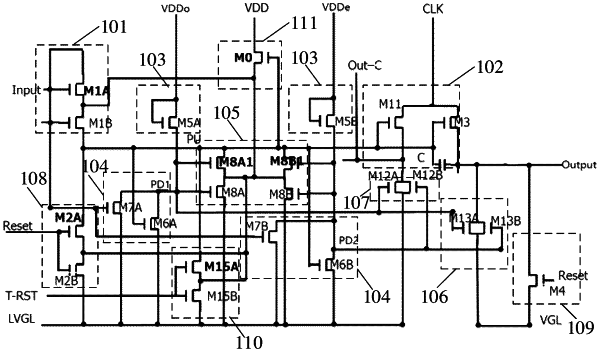
1. A shift register unit, comprising: an input sub-circuit, an output sub-circuit, at least one pull-down control sub-circuit, at least one pull-down sub-circuit, at least one first noise reduction sub-circuit, at least one second noise reduction sub-circuit, at least one third noise reduction sub-circuit, a first reset sub-circuit, a second reset sub-circuit, a shift reset sub-circuit, and a reverse bias sub-circuit; a pull-up node is at least simultaneously connected to the input sub-circuit, the output sub-circuit, and the first noise reduction sub-circuit; and a pull-down node is at least simultaneously connected to the pull-down control sub-circuit, the pull-down sub-circuit, and the first noise reduction sub-circuit; and
the input sub-circuit comprises: at least two first transistors; the output sub-circuit comprises: a third transistor, an eleventh transistor, and a storage capacitor; the pull-down control sub-circuit comprises: a fifth transistor; the pull-down sub-circuit comprises: a sixth transistor and a seventh transistor; the first noise reduction sub-circuit comprises: at least two eighth transistors; the second noise reduction sub-circuit comprises: a thirteenth transistor; the third noise reduction sub-circuit comprises: a twelfth transistor; the first reset sub-circuit comprises: at least two second transistors; the second reset sub-circuit comprises: a fourth transistor; the shift reset sub-circuit comprises: at least two fifteenth transistors; and the reverse bias sub-circuit comprises: a reverse bias control transistor;
control electrodes of the two first transistors are both connected to a signal input terminal, a first one of the first transistors has a first electrode connected to the signal input terminal, and a second electrode connected to a first electrode of a second one of the first transistors and a second electrode of the reverse bias control transistor, and a second electrode of the second one of the first transistors is connected to the pull-up node;
the third transistor has a control electrode connected to the pull-up node, a first electrode connected to a clock signal terminal, and a second electrode connected to a signal output terminal;
the eleventh transistor has a control electrode connected to the pull-up node, a first electrode connected to the clock signal terminal, and a second electrode connected to a cascade signal terminal;
one terminal of the storage capacitor is connected to the pull-up node, and the other terminal of the storage capacitor is connected to the signal output terminal;
a control electrode and a first electrode of the fifth transistor are both connected to a power voltage terminal, and a second electrode of the fifth transistor is connected to the pull-down node;
the sixth transistor has a control electrode connected to the pull-up node, a first electrode connected to a first reference level terminal, and a second electrode connected to the pull-down node;
the seventh transistor has a control electrode connected to the signal input terminal, a first electrode connected to the first reference level terminal, and a second electrode connected to the pull-down node;
control electrodes of the two eighth transistors are both connected to the pull-down node, a first one of the eighth transistors has a first electrode connected to the first reference level terminal, and a second electrode connected to a first electrode of a second one of the eighth transistors and the second electrode of the reverse bias control transistor, and a second electrode of the second one of the eighth transistors is connected to the pull-up node;
the thirteenth transistor has a control electrode connected to the pull-down node, a first electrode connected to a second reference level terminal, and a second electrode connected to the signal output terminal;
the twelfth transistor has a control electrode connected to the pull-down node, a first electrode connected to the first reference level terminal, and a second electrode connected to the cascade signal terminal;
control electrodes of the two second transistors are both connected to a reset signal terminal, a first one of the second transistors has a first electrode connected to the first reference level terminal, and a second electrode connected to a first electrode of a second one of the second transistors and the reverse bias sub-circuit, and a second electrode of the second one of the second transistors is connected to the pull-up node;
the fourth transistor has a control electrode connected to the reset signal terminal, a first electrode connected to the second reference level terminal, and a second electrode connected to the signal output terminal;
control electrodes of the two fifteenth transistors are both connected to a shift reset signal terminal, a first one of the fifteenth transistors has a first electrode connected to the first reference level terminal, and a second electrode connected to a first electrode of a second one of the fifteenth transistors and the second electrode of the reverse bias control transistor, and a second electrode of the second one of the fifteenth transistors is connected to the pull-up node; and
a control electrode of the reverse bias control transistor is connected to the pull-up node, a first electrode of the reverse bias control transistor is connected to the power voltage terminal, and the second electrode of the reverse bias control transistor is connected to the second electrode of the first one of the first transistors, the second electrode of the first one of the eighth transistors, the second electrode of the first one of the second transistors, and the second electrode of the first one of the fifteenth transistors.
|