| CPC G11C 16/24 (2013.01) [G11C 16/0483 (2013.01); H01L 24/08 (2013.01); H01L 25/0657 (2013.01); H01L 25/18 (2013.01); H01L 2224/08145 (2013.01); H01L 2225/06541 (2013.01); H01L 2924/1431 (2013.01); H01L 2924/14511 (2013.01)] | 20 Claims |
|
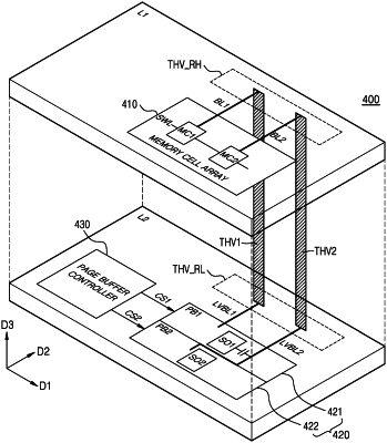
1. A nonvolatile memory device comprising:
a cell region including a first metal pad and a memory cell array, the memory cell array including a first memory cell and a second memory cell, the first memory cell being connected to a first word line and a first bit line, and the second memory cell being connected to the first word line and a second bit line; and
a peripheral circuit region including a second metal pad and vertically connected to the cell region by the first metal pad and the second metal pad,
wherein the peripheral circuit region further includes:
a page buffer circuit including a first page buffer and a second page buffer, the first page buffer being connected to the first bit line, and the second page buffer being connected to the second bit line; and
a page buffer controller configured to control the first page buffer and the second page buffer to respectively detect data values respectively stored in the first memory cell and the second memory cell, wherein a develop timing of a first sensing node of the first page buffer is different from a develop timing of a second sensing node of the second page buffer.
|