| CPC G11C 13/0069 (2013.01) [G11C 13/0028 (2013.01); G11C 13/0038 (2013.01); G11C 2013/0078 (2013.01); G11C 2213/79 (2013.01)] | 20 Claims |
|
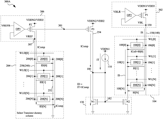
1. A memory circuit comprising:
a first driver circuit;
a memory cell array including a first column of memory cells;
a first transistor coupled between the first driver circuit and the memory cell array, the first transistor is configured to receive a first select signal;
a second driver circuit;
a first column of tracking cells configured to track a leakage current of the first column of memory cells, and coupled between a first conductive line and a second conductive line, the first conductive line being coupled to the second driver circuit; and
a header circuit coupled to the first driver circuit and the second driver circuit.
|