| CPC G11C 13/0028 (2013.01) [G11C 13/0026 (2013.01); G11C 13/003 (2013.01); G11C 13/0038 (2013.01); G11C 13/0069 (2013.01); G11C 2213/79 (2013.01)] | 20 Claims |
|
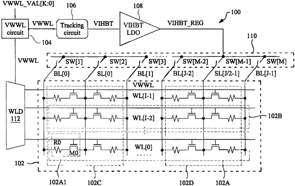
1. A memory system comprising:
a memory array;
a tracking circuit configured to receive a word line voltage provided to the memory array and to provide an inhibit voltage to bias a plurality of unselected memory cells of the memory array; and
a voltage regulator configured to receive the inhibit voltage and to provide a regulated inhibit voltage to the plurality of unselected memory cells,
wherein the tracking circuit includes:
a second voltage regulator configured to receive the word line voltage;
a resistor network coupled to a second voltage regulator to provide the inhibit voltage, wherein the resistor network comprising a plurality of resistors and wherein each of the resistors are coupled in series to an adjacent one of the plurality of resistors; and
a switch network comprising a plurality of second switches, wherein each of the second switches is coupled to a corresponding one of the plurality of resistors and to the voltage regulator.
|