| CPC G09G 3/3266 (2013.01) [G09G 3/32 (2013.01); G09G 2310/0267 (2013.01); G09G 2310/0286 (2013.01); G09G 2310/08 (2013.01); G11C 19/28 (2013.01)] | 20 Claims |
|
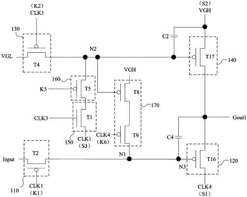
1. A shift register, comprising:
a first input circuit coupled to an input signal terminal, a first control signal terminal and a first node, wherein the first input circuit is configured to transmit an input signal provided by the input signal terminal to the first node under control of a first control signal provided by the first control signal terminal;
a first output circuit coupled to a first output signal terminal, the first node and a first scan signal terminal, wherein the first output circuit is configured to transmit a first output signal provided by the first output signal terminal to the first scan signal terminal under control of a potential of the first node;
a second input circuit coupled to a first voltage signal terminal, a second control signal terminal and a second node, wherein the second input circuit is configured to transmit a first voltage signal provided by the first voltage signal terminal to the second node under control of a second control signal provided by the second control signal terminal;
a second output circuit coupled to a second output signal terminal, the second node and the first scan signal terminal, wherein the second output circuit is configured to transmit a second output signal provided by the second output signal terminal to the first scan signal terminal under control of a potential of the second node; and
at least one functional circuit, a functional circuit being coupled to a functional input terminal, a functional output terminal and a functional control terminal, wherein the functional circuit is configured to block a path between the functional input terminal and the functional output terminal under control of a functional control signal provided by the functional control terminal, so as to maintain a potential of the functional output terminal;
wherein the functional output terminal includes one of circuit nodes.
|