| CPC G09G 3/3233 (2013.01) [G09G 3/3258 (2013.01); G09G 3/3266 (2013.01); G09G 3/3291 (2013.01); G09G 2300/0426 (2013.01); G09G 2310/0243 (2013.01)] | 20 Claims |
|
1. A pixel circuit, comprising:
a driving element including a first electrode connected to a pixel driving voltage line, a gate electrode connected to a first node, and a second electrode connected to a second node;
a first switch element configured to supply a data voltage to the first node in response to a first gate signal;
a second switch element configured to supply a reference voltage to the first node in response to a second gate signal;
a third switch element configured to supply an initialization voltage to a third node in response to a third gate signal;
a fourth switch element configured to connect the second node and the third node in response to a fourth gate signal;
a first capacitor having a first electrode connected to the first node and a second electrode connected to the second node;
a second capacitor having a first electrode connected to the pixel driving voltage line and a second electrode connected to the second node;
a third capacitor having a first electrode connected to a gate electrode of the second switch element and a second electrode connected to the second node; and
a light-emitting element having a first electrode connected to the third node and a second electrode connected to a low-potential power voltage line.
|
|
13. A pixel circuit, comprising:
a driving element including a first electrode connected to a pixel driving voltage line, a gate electrode connected to a first node, and a second electrode connected to a second node;
a first switch element configured to supply a data voltage to the first node in response to a first gate signal;
a second switch element configured to supply a reference voltage to the first node in response to a second gate signal;
a third switch element configured to supply an initialization voltage to a third node in response to a third gate signal;
a fourth switch element configured to connect the second node and the third node in response to a fourth gate signal;
a first capacitor having a first electrode connected to the first node and a second electrode connected to the second node;
a second capacitor having a first electrode connected to the pixel driving voltage line and a second electrode connected to the second node;
a fourth capacitor having a first electrode connected to the pixel driving voltage line and a second electrode connected to the first node; and
a light-emitting element first electrode connected to the third node and a second electrode connected to a low-potential power voltage line.
|
|
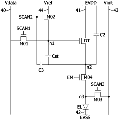
15. A display device, comprising
a display panel in which a plurality of data lines, a plurality of gate lines intersecting the data lines, a plurality of power lines through which different voltages are applied, and a plurality of pixel circuits are disposed,
wherein each of the plurality of pixel circuits includes:
a driving element including a first electrode connected to a pixel driving voltage line, a gate electrode connected to a first node, and a second electrode connected to a second node;
a first switch element configured to supply a data voltage to the first node in response to a first gate signal (SCAN1);
a second switch element configured to supply a reference voltage to the first node in response to a second gate signal (SCAN2);
a third switch element configured to supply an initialization voltage to a third node in response to a third gate signal (SCAN3);
a fourth switch element configured to connect the second node and the third node in response to a fourth gate signal (EM);
a first capacitor connected between the first node and the second node;
a second capacitor connected between the pixel driving voltage line and the second node;
a third capacitor connected between a gate electrode of the second switch element and the second node; and
a light-emitting element connected between the third node and a low-potential power voltage line.
|