| CPC G09G 3/3233 (2013.01) [G09G 2300/0426 (2013.01); G09G 2300/0819 (2013.01); G09G 2300/0842 (2013.01); G09G 2300/0861 (2013.01); G09G 2310/0262 (2013.01); G09G 2310/08 (2013.01); G09G 2320/02 (2013.01); G09G 2320/045 (2013.01)] | 13 Claims |
|
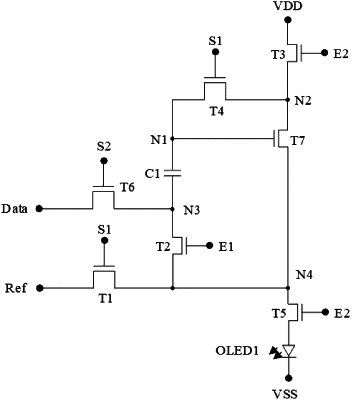
1. A pixel drive circuit, comprising: a data input circuit, a reset compensation circuit, a first switch circuit, a second switch circuit, a third switch circuit, an energy storage circuit and a light-emitting control circuit;
wherein
the data input circuit is in electrical connection with a control end of the light-emitting control circuit via the energy storage circuit, the data input circuit is configured to output a data voltage in a writing phase, and the energy storage circuit is configured to store electric energy;
the reset compensation circuit is in electrical connection with an output of the light-emitting control circuit, and the reset compensation circuit is configured to output a reset voltage in a reset compensation phase;
the first switch circuit is connected between an output of the data input circuit and an output of the reset compensation circuit, and the second switch circuit is connected between an input of the light-emitting control circuit and a first power supply, the third switch circuit is connected between the control end and the input of the light-emitting control circuit; the first switching circuit is switched on in the reset compensation phase and a light-emitting phase, and the second switching circuit is switched on in the light-emitting phase, the third switch circuit is switched on in the reset compensation phase;
the output of the light-emitting control circuit is in electrical connection with an anode of a light-emitting device, and the light-emitting control circuit is configured to output a driving current to the light-emitting device in the light-emitting phase; a cathode of the light-emitting device is in electrical connection with a second power supply; and a voltage of the second power supply is higher than or equal to the reset voltage; and
a fourth switch circuit, and an input of the fourth switch circuit is in electrical connection with the output of the reset compensation circuit and the output of the light-emitting control circuit, an output of the fourth switch circuit is in electrical connection with the anode of the light-emitting device, and the fourth switch circuit is switched on in the light-emitting phase.
|