| CPC G09G 3/32 (2013.01) [H01L 25/167 (2013.01); H01L 27/1255 (2013.01); G09G 2300/026 (2013.01); G09G 2300/0426 (2013.01); G09G 2300/0819 (2013.01); G09G 2300/0852 (2013.01); G09G 2310/066 (2013.01); G09G 2310/08 (2013.01); H01L 27/124 (2013.01)] | 25 Claims |
|
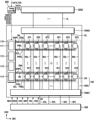
1. A display device comprising:
pulse width modulation (PWM) data lines configured to receive PWM data voltages;
first to third data lines configured to receive corresponding data voltages from among first to third data voltages;
sweep signal lines configured to receive sweep signals; and
a sub-pixel connected to a PWM data line from among the PWM data lines, a data line from among the first to third data lines, and a sweep signal line from among the sweep signal lines, and comprises at least one light emitting element,
wherein the sub-pixel further comprises:
a first transistor;
a first capacitor electrode connected to a gate electrode of the first transistor; and
a second capacitor electrode connected to the sweep signal line, and overlapping the first capacitor electrode in a thickness direction of the display device,
wherein the second capacitor electrode does not overlap a source electrode and a drain electrode of the first transistor in the thickness direction of the display device.
|