| CPC G09G 3/32 (2013.01) [G09G 2300/0842 (2013.01); G09G 2310/0286 (2013.01); G09G 2330/021 (2013.01)] | 20 Claims |
|
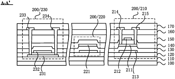
1. A display panel, comprising a substrate and a drive circuit located on one side of the substrate; wherein
the drive circuit comprises a first transistor, the first transistor comprises a first active layer, and the first active layer comprises an oxide semiconductor; and
the drive circuit further comprises a first capacitor, and one capacitor plate of the first capacitor is disposed in a same layer as the first active layer;
wherein the drive circuit comprises a pixel circuit, the pixel circuit comprises a data writing transistor, a drive transistor, and a node potential adjustment capacitor, wherein the node potential adjustment capacitor is disposed in series between a gate of the data writing transistor and a gate of the drive transistor; and the first capacitor comprises the node potential adjustment capacitor.
|