| CPC G09G 3/32 (2013.01) [G09G 3/2074 (2013.01); G09G 2300/02 (2013.01); G09G 2300/0413 (2013.01); G09G 2300/0426 (2013.01); G09G 2300/0456 (2013.01); G09G 2330/04 (2013.01)] | 17 Claims |
|
1. A display apparatus comprising:
a first sub-pixel electrode;
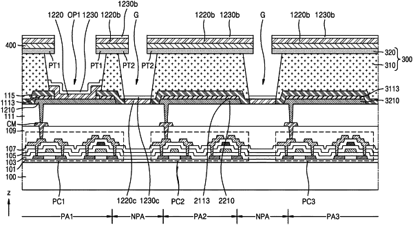
a metal bank layer in which a first opening overlapping the first sub-pixel electrode is defined, the metal bank layer including:
a first metal layer; and
a second metal layer on the first metal layer;
an insulating layer between an outer portion of the first sub-pixel electrode and the metal bank layer;
a first intermediate layer overlapping the first sub-pixel electrode through the first opening of the metal bank layer;
a first opposite electrode disposed on the first intermediate layer through the first opening of the metal bank layer; and
a low-reflective layer disposed on the second metal layer of the metal bank layer and having a reflectivity less than a reflectivity of the second metal layer, wherein the low-reflective layer includes a metal oxide and is disposed between an upper surface of the metal bank layer and a first dummy portion including a same material as a material of the first intermediate layer.
|