| CPC G09G 3/32 (2013.01) [G09G 3/30 (2013.01); G09G 3/3225 (2013.01); G09G 3/3233 (2013.01); G09G 3/3275 (2013.01); G09G 3/3266 (2013.01); G09G 2300/0426 (2013.01); G09G 2300/0842 (2013.01); G09G 2310/027 (2013.01); G09G 2310/08 (2013.01)] | 16 Claims |
|
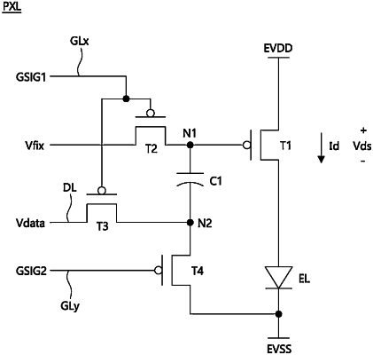
1. A display panel, comprising:
a plurality of pixels,
wherein each of the plurality of pixels comprises:
a first transistor including a gate electrode connected to a first node and a first electrode to which a high level driving voltage is for being applied;
a light emitting device including an anode electrode connected to a second electrode of the first transistor and a cathode electrode to which a low level driving voltage is for being applied;
a second transistor for supplying a predetermined fixing voltage to the first node on the basis of a first gate signal;
a third transistor for supplying a data voltage for image expression to a second node on the basis of the first gate signal;
a fourth transistor connecting the second node to an input terminal for the low level driving voltage on the basis of a second gate signal having a phase opposite to a phase of the first gate signal; and
a capacitor connected between the first node and the second node, and
wherein a level of a driving current flowing in the light emitting device during an on duty period of the light emitting device is to be constant regardless of a level of the data voltage,
wherein one frame comprises a first period and a second period succeeding the first period,
wherein during the first period, the first gate signal is to maintain an on level and the second gate signal is to maintain an off level,
wherein during the second period, the first gate signal is to maintain an off level and the second gate signal is to maintain an on level,
wherein the on duty period of the light emitting device has a length shorter than the second period, and is to vary depending on the level of the data voltage within the second period,
wherein the one frame has no more than one on-duty period of the light emitting device,
wherein the on duty period of the light emitting device is set based on a discharge speed at which the data voltage of the second node is discharged until a voltage of the capacitor is up to a threshold voltage of the first transistor, and
wherein the discharge speed for a first data voltage of a first level is faster than the discharge speed for a second data voltage of a second level which is lower than the first level.
|