| CPC G09G 3/32 (2013.01) [G06F 1/163 (2013.01); G02B 27/017 (2013.01); G02B 2027/0178 (2013.01); G09G 2300/0857 (2013.01); G09G 2310/0272 (2013.01); G09G 2310/08 (2013.01); G09G 2330/021 (2013.01); G09G 2340/04 (2013.01)] | 7 Claims |
|
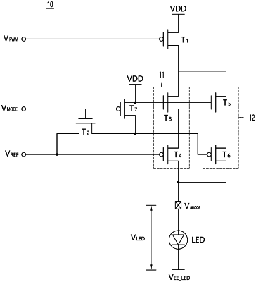
1. A pixel driving circuit comprising:
a driving line configured to connect between an output of a first transistor and a positive power source or between the output of the first transistor and a negative power source;
the first transistor connected in series on the driving line and turned on in response to a pulse width modulation (PWM) signal;
a first driving unit and a second driving unit that are connected in series from the driving line to a light emitting diode and electrically connected in parallel to each other; and
a second transistor connected between a reference voltage source and the second driving unit, wherein the reference voltage source is configured to apply a reference voltage to the first driving unit and the second driving unit,
wherein when operating in a first display mode, the first and second driving unit are turned on, and
when operating in a second display mode, the first driving unit is turned on for a cyclic period comprising first and second portion periods, and the second transistor is configured to turn on the second driving unit for the first portion period and turn off the second driving unit for the second portion period,
wherein the second display mode has a higher resolution than the first display mode,
wherein
the first driving unit includes:
a third transistor connected in series on the driving line and turned on in response to the positive power source; and
a fourth transistor connected in series on the driving line and turned on in response to the reference voltage, and
the second driving unit includes:
a fifth transistor connected in series on the driving line and turned on in response to the positive power source; and
a sixth transistor connected in series on the driving line and turned on in response to the reference voltage when the second transistor is turned on.
|