| CPC G06T 7/001 (2013.01) [G06N 3/045 (2023.01); G06T 7/11 (2017.01); G06T 7/97 (2017.01); G06T 2207/10024 (2013.01); G06T 2207/10061 (2013.01); G06T 2207/20081 (2013.01); G06T 2207/20084 (2013.01); G06T 2207/20221 (2013.01); G06T 2207/30148 (2013.01)] | 20 Claims |
|
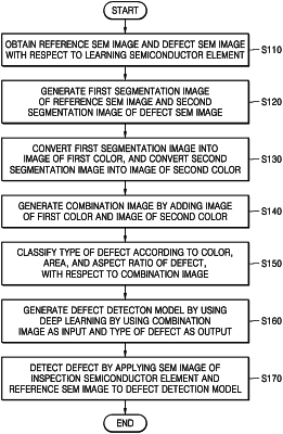
1. A deep learning-based defect detection method for a semiconductor element, the defect detection method comprising:
generating a first segmentation image from a reference scanning electron microscope (SEM) image without a defect and a second segmentation image from a defect SEM image with the defect, with respect to a learning semiconductor element;
converting the first segmentation image into an image of a first color among a red color, a green color, or a blue color, and converting the second segmentation image into an image of a second color, different from the first color, among the red color, the green color, or the blue color;
generating a combination image by adding the image of the first color and the image of the second color;
classifying a type of the defect in the learning semiconductor element according to at least one among a color and an aspect ratio of the defect, with respect to the combination image;
generating, using deep learning, a defect detection model using the combination image as an input and the type of the defect as an output; and
detecting a defect in an inspection semiconductor element by applying an SEM image of the inspection semiconductor element and the reference SEM image to the defect detection model,
wherein the first segmentation image and the second segmentation image correspond to SEM images of a segmentation region, in which an intensity difference between the reference SEM image and the defect SEM image is higher than a reference value.
|