| CPC G06F 30/398 (2020.01) [G03F 1/36 (2013.01); G03F 1/70 (2013.01); H03H 11/20 (2013.01)] | 20 Claims |
|
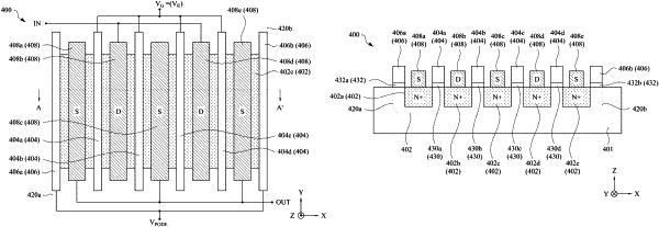
1. A phase shifter comprising:
a first transistor comprising:
a first gate terminal configured to receive a first voltage, the first transistor configured to adjust at least a resistance or a first capacitance of the phase shifter responsive to the first voltage; and
a second transistor coupled to the first transistor, the second transistor comprising:
a second gate terminal configured to receive a second voltage, the second transistor configured to adjust a second capacitance of the phase shifter responsive to the second voltage, the second gate terminal including a first polysilicon portion and a second polysilicon portion extending in a first direction, and the first polysilicon portion and the second polysilicon portion being positioned along opposite edges of an active region of the first transistor and the second transistor.
|