US 12,229,487 B2
Hotspot avoidance method of manufacturing integrated circuits
I-Shuo Liu, Hsinchu (TW); Chih-Chun Hsia, Hsinchu (TW); Hsin-Ting Chou, Hsinchu (TW); Kuanhua Su, Hsinchu (TW); William Weilun Hong, Hsinchu (TW); Chih Hung Chen, Hsinchu (TW); and Kei-Wei Chen, Tainan (TW)
Assigned to TAIWAN SEMICONDUCTOR MANUFACTURING CO., LTD., Hsinchu (TW)
Filed by Taiwan Semiconductor Manufacturing Co., Ltd., Hsinchu (TW)
Filed on Apr. 28, 2023, as Appl. No. 18/308,916.
Application 18/308,916 is a continuation of application No. 17/814,991, filed on Jul. 26, 2022, granted, now 11,675,953.
Application 17/814,991 is a continuation of application No. 16/926,026, filed on Jul. 10, 2020, granted, now 11,443,095, issued on Sep. 13, 2022.
Prior Publication US 2023/0267264 A1, Aug. 24, 2023
Int. Cl. G06F 30/392 (2020.01); G06F 111/20 (2020.01); G06T 7/00 (2017.01)
CPC G06F 30/392 (2020.01) [G06T 7/001 (2013.01); G06F 2111/20 (2020.01); G06T 2207/20021 (2013.01); G06T 2207/30148 (2013.01)] 20 Claims
OG exemplary drawing
 
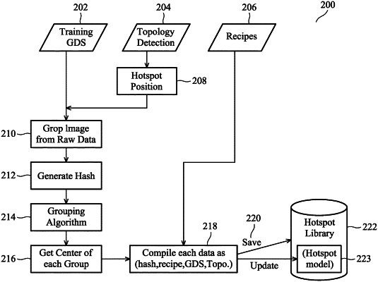
1. A method comprising:
determining likely hotspots of a wafer;
comparing hash values of the likely hotspots with stored hash values in a hotspot library to determine a similarity value for each of the likely hotspots; and
based on the similarity values determined in the comparing, selecting a polishing recipe from the hotspot library.