| CPC G06F 3/0659 (2013.01) [G06F 3/0604 (2013.01); G06F 3/0679 (2013.01); G11C 16/0483 (2013.01); G11C 16/26 (2013.01)] | 14 Claims |
|
1. A semiconductor memory device comprising:
a first pad;
a second pad;
a first memory string comprising a plurality of first memory cell transistors connected in series;
a first bit line connected to one end of the first memory string;
a first source line connected to the other end of the first memory string;
a plurality of first word lines connected to gates of the first memory cell transistors, respectively:
a first sense amplifier connected to the first bit line;
a first data register connected to the first sense amplifier and configured to store data read from one of the first memory cell transistors; and
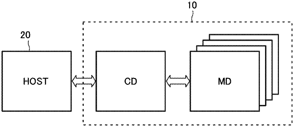
a control circuit configured to execute an operation in response to instruction from an external memory controller through the second pad, wherein
in response to a first command instructing data output through the second pad, the data stored in the first data register is output toward the external memory controller from the first pad, and
in response to a second command instructing status output through the second pad, status information is output toward the external memory controller from the second pad.
|