| CPC G06F 3/0655 (2013.01) [G06F 3/0604 (2013.01); G06F 3/0679 (2013.01); G06F 13/1668 (2013.01); G11C 7/06 (2013.01); G11C 7/1057 (2013.01); G11C 7/106 (2013.01); G11C 7/1066 (2013.01); G11C 7/1087 (2013.01); G11C 7/1093 (2013.01); G11C 7/22 (2013.01); G11C 11/4076 (2013.01); G11C 11/4096 (2013.01); H01L 25/0657 (2013.01); G06F 2213/16 (2013.01); G11C 7/1015 (2013.01); G11C 2207/107 (2013.01); G11C 2207/2272 (2013.01); G11C 2207/2281 (2013.01); G11C 2207/229 (2013.01); H01L 2225/06541 (2013.01)] | 20 Claims |
|
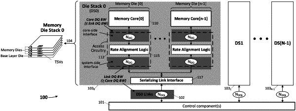
1. A stacked-die memory component to be coupled to a processing component, the stacked-die memory component comprising:
a plurality of memory dies disposed in a stack; and
a base die having (i) a first interface coupled to receive, from any one of the memory dies, successive sets of N data bits over successive memory-die readout intervals, respectively, N being a nonzero integer, and (ii) a second interface to output the successive sets of N data bits to the processing component over successive data-output intervals, respectively, each one of the data-output intervals being briefer than any one of the memory-die readout intervals.
|