US 12,229,360 B2
Display panel and display touch-control apparatus
Chang Luo, Beijing (CN); Xiping Li, Beijing (CN); Hongwei Ma, Beijing (CN); Ming Hu, Beijing (CN); Wei He, Beijing (CN); Youngyik Ko, Beijing (CN); Haijun Qiu, Beijing (CN); Yi Zhang, Beijing (CN); Taofeng Xie, Beijing (CN); Tianci Chen, Beijing (CN); Qun Ma, Beijing (CN); Xinghua Li, Beijing (CN); Ping Wen, Beijing (CN); Yang Zhou, Beijing (CN); Yuanqi Zhang, Beijing (CN); Xiaoyan Yang, Beijing (CN); Shun Zhang, Beijing (CN); Pandeng Tang, Beijing (CN); Yang Zeng, Beijing (CN); Tong Zhang, Beijing (CN); Xiaofei Hou, Beijing (CN); Zhidong Wang, Beijing (CN); Haoyuan Fan, Beijing (CN); and Jinhwan Hwang, Beijing (CN)
Assigned to Chengdu BOE Optoelectronics Technology Co., Ltd., Sichuan (CN); and BOE Technology Group Co., Ltd., Beijing (CN)
Appl. No. 18/281,963
Filed by Chengdu BOE Optoelectronics Technology Co., Ltd., Sichuan (CN); and BOE Technology Group Co., Ltd., Beijing (CN)
PCT Filed Jan. 9, 2023, PCT No. PCT/CN2023/071199
§ 371(c)(1), (2) Date Sep. 14, 2023,
PCT Pub. No. WO2023/142988, PCT Pub. Date Aug. 3, 2023.
Claims priority of application No. 202210112870.2 (CN), filed on Jan. 29, 2022.
Prior Publication US 2024/0160306 A1, May 16, 2024
Int. Cl. G06F 3/041 (2006.01); G06F 3/044 (2006.01)
CPC G06F 3/0412 (2013.01) [G06F 3/04164 (2019.05); G06F 3/0445 (2019.05); G06F 3/0446 (2019.05)] 18 Claims
OG exemplary drawing
 
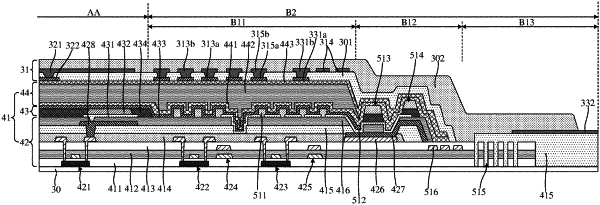
1. A display panel comprising: an active area, a peripheral area located at a periphery of the active area; wherein
the active area comprises a base substrate, a display structure layer and a touch structure layer arranged sequentially on the base substrate;
the peripheral area comprises an isolation dam, a first ground trace and a second ground trace arranged on the base substrate; and
the first ground trace is located on a side of the isolation dam close to the active area, and the second ground trace is located on a side of the isolation dam away from the active area,
wherein the touch structure layer comprises: a first touch conductive layer, a first touch insulating layer, a second touch conductive layer, and a second touch insulating layer arranged sequentially on the display structure layer; and
the first ground trace and the second ground trace are of a structure of a same layer as the second touch conductive layer,
wherein an orthographic projection of the second touch insulating layer on the base substrate partially overlaps an orthographic projection of the second ground trace on the base substrate.