| CPC G06F 13/20 (2013.01) [G06F 1/10 (2013.01)] | 20 Claims |
|
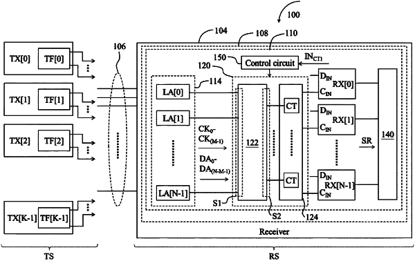
1. An integrated circuit in a transmitter, the integrated circuit comprising:
a multi-lane interface having N lanes, N being an integer greater than one;
N signal generating circuits, coupled to the multi-lane interface, wherein M of the N signal generating circuits are configured to generate M clock signals respectively, and (N-M) of the N signal generating circuits are configured to generate (N-M) data signals respectively, M being a positive integer less than N;
a control circuit, configured to generate a set of selection signals according to a control input, the control input being indicative of respective lane identifiers of M of the N lanes, each of the M lanes being coupled to a clock lane of a receiver, the clock lane of the receiver being arranged for receiving one of the M clock signals; and
a lane selection circuit, coupled between the multi-lane interface and the N signal generating circuits, the lane selection circuit being controlled by the set of selection signals to distribute the M clock signals and the (N-M) data signals to the N lanes, wherein the lane selection circuit is configured to select the M lanes as M clock lanes by coupling the M clock signals to the M lanes respectively, and couple the (N-M) data signals to remaining (N-M) lanes respectively, wherein the remaining (N-M) lanes serve as (N-M) data lanes.
|