US 12,229,000 B2
Managing error-handling flows in memory devices
Kishore Kumar Muchherla, San Jose, CA (US); Shane Nowell, Boise, ID (US); Mustafa N. Kaynak, San Diego, CA (US); Sampath K. Ratnam, San Jose, CA (US); Peter Feeley, Boise, ID (US); Sivagnanam Parthasarathy, Carlsbad, CA (US); Devin M. Batutis, San Jose, CA (US); and Xiangang Luo, Fremont, CA (US)
Assigned to Micron Technology, Inc., Boise, ID (US)
Filed by Micron Technology, Inc., Boise, ID (US)
Filed on Jun. 8, 2023, as Appl. No. 18/207,525.
Application 18/207,525 is a continuation of application No. 17/216,901, filed on Mar. 30, 2021, granted, now 11,709,727.
Prior Publication US 2023/0325273 A1, Oct. 12, 2023
Int. Cl. G06F 11/00 (2006.01); G06F 11/07 (2006.01)
CPC G06F 11/0793 (2013.01) [G06F 11/0727 (2013.01); G06F 11/0751 (2013.01)] 20 Claims
OG exemplary drawing
 
1. A system comprising:
a memory device; and
a processing device, operatively coupled to the memory device, to perform operations comprising:
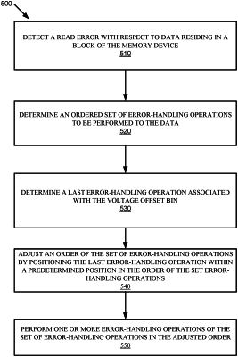
detecting a read error with respect to data residing in a first block of the memory device, wherein the first block is assigned to a voltage offset bin which defines a set of threshold voltage offsets to be applied to a base voltage read level during read operations;
determining a most recently performed error-handling operation performed on a second block associated with the voltage offset bin; and
performing the error-handling operation to recover the data.