| CPC G02F 1/13394 (2013.01) [G02F 1/136286 (2013.01); H01L 27/124 (2013.01); G02F 2201/121 (2013.01); G02F 2202/02 (2013.01)] | 18 Claims |
|
1. An array substrate, comprising:
a first substrate;
a transistor, formed on the first substrate;
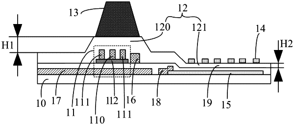
an organic insulation layer, formed on the first substrate and covering the transistor;
a spacer, formed on a side of the organic insulation layer away from the first substrate, wherein, an orthographic projection of the spacer on the first substrate at least partially overlaps with an orthographic projection of the transistor on the first substrate, the spacer is in direct contact with a portion of the organic insulation layer covering the transistor and provided with a greater thickness than other portion of the organic insulation layer; and
a pixel electrode, wherein the pixel electrode comprises a first portion and a second portion arranged in a column direction and integrally formed; the first portion comprises a first electrode strip and a first slit alternately arranged in the column direction; the second portion comprises a second electrode strip and a second slit alternately arranged in the column direction; the first electrode strip and the first slit extend along a third direction; the second electrode strip and the second slit extend along a fourth direction; the third direction and the fourth direction intersect with each other and are mirror symmetric with respect to a row direction; and the first slit and the second slit are closed at both ends of their extending direction in regions other than at least an intermediate region where the first portion and the second portion meet;
a common line, extending in the row direction, the common line and a gate of the transistor are arranged on a same layer, an orthographic projection of the common line on the first substrate does not overlap with an orthographic projection of the gate of the transistor on the first substrate;
a data line, extending in a column direction, wherein the data line is connected to a second electrode of the transistor; and
a scanning line, extending in a row direction, wherein the scanning line is connected to a gate of the transistor;
wherein the orthographic projection of the spacer on the first substrate at least partially overlaps with an orthographic projection of the data line on the first substrate, and at least partially overlaps with an orthographic projection of the scanning line on the first substrate.
|