| CPC G02B 6/124 (2013.01) [B29D 11/00663 (2013.01); G02B 6/1228 (2013.01); G02B 6/132 (2013.01); G02B 2006/12097 (2013.01); G02B 2006/12107 (2013.01); G02B 2006/12197 (2013.01)] | 20 Claims |
|
1. A method, comprising:
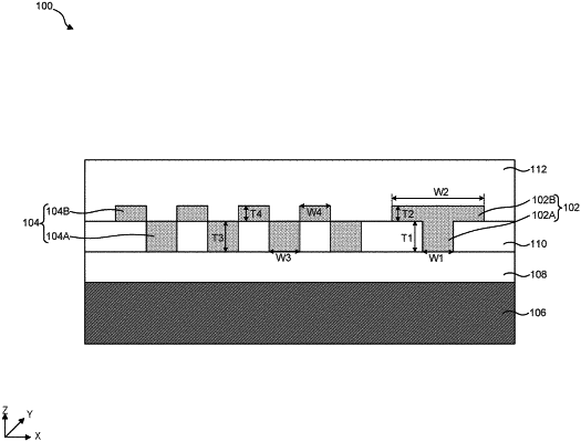
forming an unpatterned thermal oxide layer on a substrate;
depositing a non-thermal oxide layer comprising a first refractive index on the unpatterned thermal oxide layer;
patterning the non-thermal oxide layer to form a trench on the unpatterned thermal oxide layer;
forming a first portion of a waveguide, in the trench, with a material comprising a second refractive index that is greater than the first refractive index;
forming a second portion of the waveguide on a top surface of the non-thermal oxide layer; and
depositing a cladding layer on the second portion of the waveguide.
|