| CPC G01N 21/211 (2013.01) [G01N 21/9501 (2013.01); G02B 27/10 (2013.01); G01N 2021/214 (2013.01)] | 19 Claims |
|
1. A method of fabricating a semiconductor device, the method comprising:
preparing the semiconductor device to be measured;
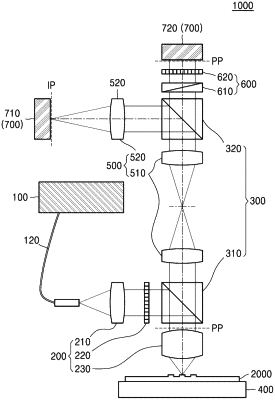
acquiring a hologram image of the semiconductor device by a pupil ellipsometry measurement apparatus;
reconstructing reflectance information based on the hologram image;
measuring the semiconductor device based on the reflectance information;
determining whether the semiconductor device is normal based on a result of the measuring; and
performing a subsequent process on the semiconductor device based on the semiconductor device being determined to be normal,
wherein the acquiring of the hologram image comprises:
producing interference light through self-interference of reflected light from the semiconductor device by a self-interference generator (SIG) included in the pupil ellipsometry measurement apparatus; and
detecting the hologram image of the interference light on a pupil plane by a first detector included in the pupil ellipsometry measurement apparatus.
|