| CPC B81B 7/007 (2013.01) [B81C 1/00301 (2013.01); B81B 2201/0271 (2013.01); B81B 2203/0127 (2013.01); B81B 2207/012 (2013.01); B81B 2207/07 (2013.01); B81B 2207/097 (2013.01); B81C 2203/0792 (2013.01)] | 20 Claims |
|
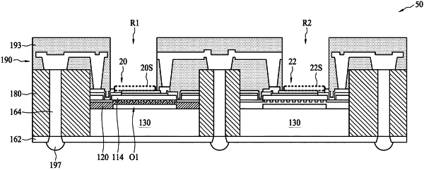
1. A method of manufacturing a semiconductor device, comprising:
providing a substrate;
disposing a first device and a second device on the substrate;
forming a sacrificial layer over the first device and the second device;
forming a conductive pillar over the substrate;
forming a molding over the substrate and surrounding the first device, the second device, the conductive pillar and the sacrificial layer;
removing some portions of the molding to expose the sacrificial layer and the conductive pillar;
removing the sacrificial layer;
forming a redistribution layer (RDL) over the first device, the second device, the molding and the conductive pillar, wherein the RDL electrically connects the first device to the second device; and
forming an opening extending through the RDL to expose a sensing area of the first device.
|