| CPC A61B 5/02438 (2013.01) [A61B 5/681 (2013.01); G06F 1/163 (2013.01); H01L 31/101 (2013.01)] | 20 Claims |
|
1. An electronic device, comprising:
a housing defining an aperture and at least partially defining an internal volume of the electronic device;
a first electromagnetic radiation emitter disposed in the internal volume;
a second electromagnetic radiation emitter disposed in the internal volume;
an electromagnetic radiation detector disposed in the internal volume;
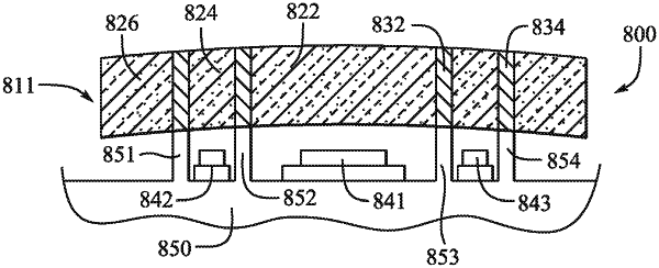
an optical component disposed in the aperture, the optical component comprising:
a first transparent portion disposed above the first electromagnetic radiation emitter;
a second transparent portion disposed above the second electromagnetic radiation emitter;
a third transparent portion disposed above the electromagnetic radiation detector; and
a first opaque portion surrounding the first transparent portion, a second opaque portion surrounding the second transparent portion, the first and second opaque portions comprising sidewalls, the first transparent portion, the second transparent portion, the third transparent portion, and the first and second opaque portions defining a flush exterior surface of the electronic device and an interior surface of the optical component, the first and second opaque portions extending from the exterior surface to the interior surface;
a first isolation protrusion disposed in the internal volume between a first chamber and a second chamber, the first isolation protrusion abutting the optical component and at least partially defining the first chamber and the second chamber; and
a second isolation protrusion disposed in the internal volume between the first chamber and a third chamber, the second isolation protrusion abutting the optical component and at least partially defining the first chamber and the third chamber;
wherein:
the first electromagnetic radiation emitter is disposed in the first chamber, the second electromagnetic radiation emitter is disposed in the second chamber, and the electromagnetic radiation detector is disposed in the third chamber;
the first isolation protrusion and the second isolation protrusion prevent electromagnetic radiation from passing between the first chamber, the second chamber, and the third chamber within the internal volume; and
the first isolation protrusion comprises sidewalls aligned with the sidewalls of the first and second opaque portions and the second isolation protrusion comprises sidewalls aligned with the sidewalls of the first and third opaque portions.
|