| CPC H10N 50/80 (2023.02) [G11C 11/161 (2013.01); G11C 11/1657 (2013.01); G11C 11/1673 (2013.01); G11C 11/1675 (2013.01); H10B 61/10 (2023.02); H10N 50/01 (2023.02); H10N 50/10 (2023.02)] | 20 Claims |
|
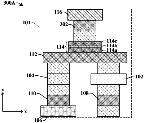
1. A memory device comprising:
a spin orbit torque (SOT) layer;
a magnetic tunnel junction (MTJ) structure over the SOT layer;
a first conductive wire below the SOT layer and coupled to the SOT layer;
a second conductive wire over the MTJ structure; and
a selector structure between the first conductive wire and the SOT layer;
wherein the first and second conductive wires have individual lengths extending laterally in parallel, and wherein a bottommost surface of the selector structure overlies a topmost surface of the first conductive wire.
|