| CPC H10N 50/80 (2023.02) [G11C 11/161 (2013.01); G11C 11/1659 (2013.01); H10B 61/22 (2023.02); G11C 11/1673 (2013.01); G11C 11/1675 (2013.01); H10N 50/85 (2023.02)] | 11 Claims |
|
1. A memory device, comprising:
a substrate;
a plurality of active areas extending along a first direction on the substrate;
a gate line traversing the active areas and extending along a second direction that is not parallel to the first direction;
a plurality of source doped regions in the active areas and on a first side of the gate line, wherein the plurality of source doped regions are substantially aligned along the second direction;
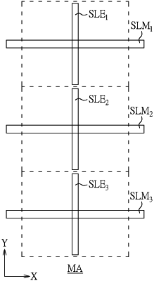
a main source line extending along the first direction;
a source line extension coupled to the main source line and extending along the second direction, wherein the source line extension elongates from opposite side edges of the main source line and electrically connects the plurality of source doped regions with the main source line;
a plurality of drain doped regions in the active areas and on a second side of the gate line that is opposite to the first side; and
a plurality of data storage elements electrically coupled to the drain doped regions, respectively.
|