| CPC H10K 85/636 (2023.02) [C07D 495/04 (2013.01); H10K 85/633 (2023.02); H10K 50/115 (2023.02); H10K 50/156 (2023.02); H10K 85/626 (2023.02); H10K 85/6572 (2023.02); H10K 85/6576 (2023.02)] | 10 Claims |
|
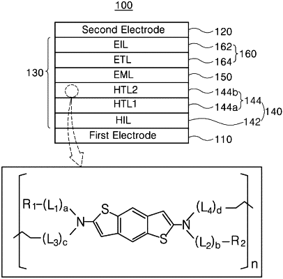
1. A light-emitting diode, comprising:
a first electrode;
a hole injection layer;
a hole transport layer;
an emitting material layer;
an electron transport layer; and
a second electrode,
wherein the hole transport layer comprises a cross-linked compound derived from a compound having the following structure of Formula 1:
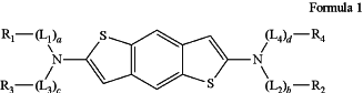 wherein:
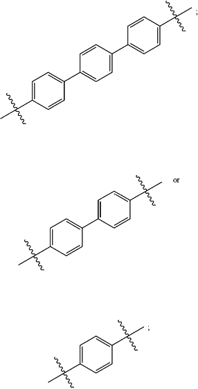
R1 and R2 are each independently
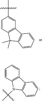 R3 and R4 are each independently
 L1, L2, L3, and L4 are each independently
 a and b are each independently 0 or 1;
c and d are each independently 1 or 2, and
wherein:
the hole injection layer consists of poly(ethylenedioxythiophene):polystyrenesulfonate;
the hole transport layer comprises:
a first hole transport layer over the hole injection layer, and
a second hole transport layer over the first hole transport layer; and
the second hole transport layer consists of the cross-linked compound.
|