| CPC H10K 71/00 (2023.02) [H10K 50/125 (2023.02); H10K 59/121 (2023.02)] | 20 Claims |
|
1. A method of fabricating a display, wherein the display comprises a full-color organic light emitting diode (OLED) display, the method comprising:
obtaining a substrate having a non-emissive insulating layer that defines active pixel areas on the substrate; and
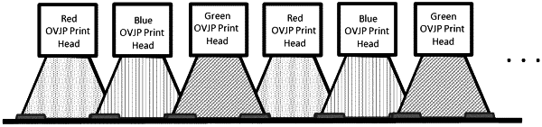
depositing, via a first organic vapor jet printing (OVJP) print head, a first organic emissive material over the substrate in a continuous line extending from a first edge of an active display portion of the substrate to a second edge of the active display portion of the substrate and being deposited over at least a portion of the non-emissive insulating layer and over at least a first portion of the active pixel areas; and
depositing, via the first OVJP print head or a second OVJP print head, a second organic emissive material different than the first organic emissive material in a continuous line extending from the first edge of the active display portion of the substrate to the second edge of the active display portion of the substrate and over at least the portion of the non-emissive insulating layer that is the same as the portion over which the first organic emissive material is deposited, and over at least a second portion of the active pixel areas that is different than the first portion.
|