| CPC H10K 59/88 (2023.02) [H10K 50/844 (2023.02); H10K 59/124 (2023.02)] | 16 Claims |

|
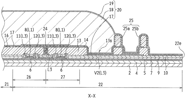
1. A display device comprising:
a substrate;
a stack of a flattening film, a first electrode, an edge cover, and a second electrode, the stack being disposed on the substrate;
a sealing layer disposed on the second electrode, the sealing layer including a first insulating sealing film, an organic film, and a second insulating sealing film;
a display region; and
a frame region surrounding the display region,
wherein the display region includes a pixel circuit including a plurality of transistors,
the frame region includes
a trench disposed in the flattening film so as to surround the display region,
a first conductive film electrically connected to the second electrode in the trench, the first conductive film being made of a material identical to a material of the first electrode, the first conductive film being disposed in a layer identical to a layer where the first electrode is disposed,
a barrier wall defining an end of the organic film so as to surround an outside of the trench,
a TEG pattern disposed between the display region and the trench, and
a dummy pixel circuit disposed between the display region and the barrier wall, the dummy pixel circuit having a configuration identical to a configuration of the pixel circuit, the dummy pixel circuit including a transistor, and
the TEG pattern is adjacent to at least the dummy pixel circuit.
|